Showing posts with label future of technology. Show all posts
Showing posts with label future of technology. Show all posts
Friday, October 11, 2013

Monday, September 30, 2013
Researchers Demonstrate 'Accelerator on a Chip'
Menlo Park, Calif. — In an advance that could dramatically shrink particle accelerators for science and medicine, researchers used a laser to accelerate electrons at a rate 10 times higher than conventional technology in a nanostructured glass chip smaller than a grain of rice.
The achievement was reported today in Nature by a team including scientists from the U.S. Department of Energy’s (DOE) SLAC National Accelerator Laboratory and Stanford University.
“We still have a number of challenges before this technology becomes practical for real-world use, but eventually it would substantially reduce the size and cost of future high-energy particle colliders for exploring the world of fundamental particles and forces,” said Joel England, the SLAC physicist who led the experiments. “It could also help enable compact accelerators and X-ray devices for security scanning, medical therapy and imaging, and research in biology and materials science.”
Because it employs commercial lasers and low-cost, mass-production techniques, the researchers believe it will set the stage for new generations of "tabletop" accelerators.
At its full potential, the new “accelerator on a chip” could match the accelerating power of SLAC’s 2-mile-long linear accelerator in just 100 feet, and deliver a million more electron pulses per second.
This initial demonstration achieved an acceleration gradient, or amount of energy gained per length, of 300 million electronvolts per meter. That's roughly 10 times the acceleration provided by the current SLAC linear accelerator.
“Our ultimate goal for this structure is 1 billion electronvolts per meter, and we’re already one-third of the way in our first experiment,” said Stanford Professor Robert Byer, the principal investigator for this research.
This animation explains how the accelerator on a chip uses infrared laser light to accelerate electrons to increasingly higher energies. (Greg Stewart/SLAC)
How It Works
Today’s accelerators use microwaves to boost the energy of electrons. Researchers have been looking for more economical alternatives, and this new technique, which uses ultrafast lasers to drive the accelerator, is a leading candidate.
Particles are generally accelerated in two stages. First they are boosted to nearly the speed of light. Then any additional acceleration increases their energy, but not their speed; this is the challenging part.
In the accelerator-on-a-chip experiments, electrons are first accelerated to near light-speed in a conventional accelerator. Then they are focused into a tiny, half-micron-high channel within a fused silica glass chip just half a millimeter long. The channel had been patterned with precisely spaced nanoscale ridges. Infrared laser light shining on the pattern generates electrical fields that interact with the electrons in the channel to boost their energy. (See the accompanying animation for more detail.)
Turning the accelerator on a chip into a full-fledged tabletop accelerator will require a more compact way to get the electrons up to speed before they enter the device.
A collaborating research group in Germany, led by Peter Hommelhoff at Friedrich Alexander Universityand the Max Planck Institute of Quantum Optics, has been looking for such a solution. Itsimultaneously reports in Physical Review Letters its success in using a laser to accelerate lower-energy electrons.
Multi-Use Accelerators
Applications for these new particle accelerators would go well beyond particle physics research. Byer said laser accelerators could drive compact X-ray free-electron lasers, comparable to SLAC’s Linac Coherent Light Source, that are all-purpose tools for a wide range of research.
Another possible application is small, portable X-ray sources to improve medical care for people injured in combat, as well as provide more affordable medical imaging for hospitals and laboratories. That’s one of the goals of the Defense Advanced Research Projects Agency’s (DARPA) Advanced X-Ray Integrated Sources (AXiS) program, which partially funded this research. Primary funding for this research is from the DOE’s Office of Science.
SLAC's Joel England explains how the same fabrication techniques used for silicon computer microchips allowed their team to create the new laser-driven particle accelerator chips. (SLAC)
The study's lead authors were Stanford graduate students Edgar Peralta and Ken Soong. Peralta created the patterned fused silica chips in the Stanford Nanofabrication Facility. Soong implemented the high-precision laser optics for the experiment at SLAC’s Next Linear Collider Test Accelerator. Additional contributors included researchers from the University of California-Los Angeles and Tech-X Corp. in Boulder, Colo.
SLAC is a multi-program laboratory exploring frontier questions in photon science, astrophysics, particle physics and accelerator research. Located in Menlo Park, California, SLAC is operated by Stanford University for the U.S. Department of Energy Office of Science. To learn more, please visitwww.slac.stanford.edu.
DOE’s Office of Science is the single largest supporter of basic research in the physical sciences in the United States, and is working to address some of the most pressing challenges of our time. For more information, please visit science.energy.gov.
Citation: E. A. Peralta et al., Nature, 27 Sept 2013 (10.1038/nature12664)
Press Office Contact: Andy Freeberg, SLAC, afreeberg@slac.stanford.edu, (650) 926-4359
Scientist Contacts:
Press Office Contact: Andy Freeberg, SLAC, afreeberg@slac.stanford.edu, (650) 926-4359
Scientist Contacts:
Robert Byer, Stanford University, rlbyer@stanford.edu, (650) 723-0226
*This post was taken from http://www6.slac.stanford.edu/news/2013-09-27-accelerator-on-a-chip.aspx*
Dental implants that heal faster and fight infection
[+]
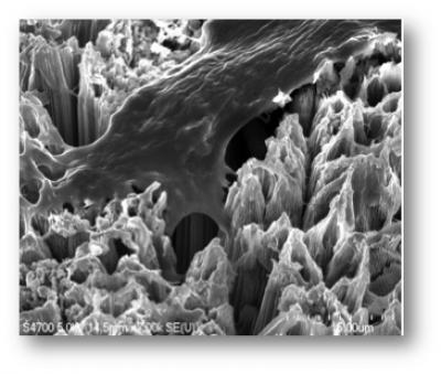
A bone cell anchoring itself to a surface of titanium dioxide nanotubes. Because osteoblasts (cells that synthesize bone tissue).readily adhere to this novel surface, dental implants coated with TiO2 nanotubes could significantly improve healing following dental implant surgery. (Credit: Tolou Shokuhfar/Michigan Technological University)
Michigan Technological University researchers have developed a way to use self-assembled titanium dioxide (TiO2) nanotubes to lower the rate of dental-implant failures.
Dental implants are posts, usually made of titanium, that are surgically placed into the jawbone and topped with artificial teeth.
While most dental implants are successful, a small percentage fail and either fall out or must be removed.
“There are two main issues that concern dentists: infection and separation from the bone,” said Tolou Shokuhfar, an assistant professor of mechanical engineering.
The mouth is a dirty place, so bacterial infections are a risk after implant surgery, and sometimes bone fails to heal securely around the device.
Because jawbones are somewhat thin and delicate, replacing a failed implant can be difficult, not to mention expensive. Generally, dentists charge between $2,000 and $4,000 to install a single implant, and the procedure is rarely covered by insurance.
[+]
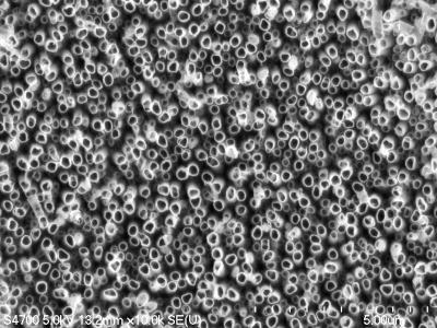
A forest of titanium dioxide nanotubes etched into metallic titanium. The surface may improve the longevity of dental implants. (Credit: Tolou Shokuhfar/Michigan Technological University)
Shokuhfar is now working with Cortino Sukotjo, a clinical assistant professor at the University of Illinois at Chicago (UIC) College of Dentistry on a dental implant with a surface made from TiO2 nanotubes, but she has been making and testing them for several years.
“We have done toxicity tests on the nanotubes, and not only did they not kill cells, they encouraged growth,” she said.
She has already demonstrated that bone cells grow more vigorously and adhere better to titanium coated with TiO2 nanotubes than to conventional titanium surfaces. That could keep more dental implants in place.
Drug delivery
The nanotubes can also be a drug delivery system. Shokuhfar’s team, in collaboration with Alexander Yarin, a professor in UIC’s Department of Mechanical and Industrial Engineering, loaded TiO2 nanotubes with the anti-inflammatory drug sodium naproxen and demonstrated that it could be released gradually after implant surgery.
That assures that the medicine gets where it’s needed, and it reduces the chances of unpleasant side effects that arise when a drug is injected or taken orally.
[+]

This cutaway view of a titanium dioxide nanotube reveals the drug sodium naproxen on the inside. On the surface of a dental implant, these nanotubes could release this anti-inflammatory drug or other pharmaceuticals that could speed healing. (Credit: Tolou Shokuhfar/Michigan Technological University)
To fight infection, the TiO2 nanotubes can also be laced with silver nanoparticles. Shokuhfar and Craig Friedrich, who holds the Richard and Bonnie Robbins Chair of Sustainable Design and Manufacturing at Michigan Tech, are conducting research, as yet unpublished, that is focused on orthopedic implants, such as artificial hips, but which also applies to dental implants.
“Silver has antimicrobial properties, and we are capable of obtaining a dose that can kill microbes but would not hurt healthy cells and tissues,” she said. In particular, it can help prevent biofilms, vast colonies of bacteria that can cover implants and be very difficult to eradicate. A nanotextured implant surface embedded with silver nanoparticles could prevent infection for the life of the implant.
The TiO2 nanotubes also have a cosmetic advantage: transparency. That’s a plus for any dental implant, but especially for a new type made from zirconia, which some patients choose because it is totally white.
Shokuhfar expects that implants with the new nanotubular surface will be easily assimilated into the market, since titanium implants, both dental and orthopedic, have a long history.
Shokuhfar and Friedrich have received a provisional patent and are working with two hospitals to further develop the technology and eventually license it. “As soon as the related paper work is taken care of and we get the FDA approval, the technology could be applied. However I am not aware how long all that would take,” she told KurzweilAI.

Interview with Dr. Tolou Shokuhfar (credit: DNN)
REFERENCES:
- Tolou Shokuhfar et al., Intercalation of anti-inflammatory drug molecules within TiO2 nanotubes, RSC Advances, 2013, DOI: 10.1039/C3RA42173B
- T. Shokuhfar et al., Biophysical Evaluation of Osteoblasts on TiO2 Nanotubes, Nanomedicine: Nanotechnology, Biology, and Medicine, 2011, Under Revision
- Patent: US 2013/0196128, COMPOSITIONS, METHODS AND DEVICES FOR GENERATING NANOTUBES ON A SURFACE
*All credit for this post goes to: http://www.kurzweilai.net/dental-implants-that-heal-faster-and-fight-infection *
Thursday, August 22, 2013
Wednesday, August 21, 2013
Sunday, June 23, 2013
End of Moore's Law
-->
According to Moores Law the
number of transistors on a integrated circuit doubles approximately every two
years (18 months). Gordron E. Moore described his law in this 1965 paper ‘Cramming more components onto integrated
circuits’ in the Electronics Magazine.
Because of this exponential growth over the last 48 years, this doubling has lead to 24 doublings of the orginal number of transitors that could be placed on a circuit board. Moore’s law is
starting to buckle, because transistors based on semiconductors can only get so
small.
"At the rate the current
technology is progressing, in 10 or 20 years, they won't be able to get any
smaller," said physicist Yoke Khin Yap of Michigan Technological
University. Not only is the current technology starting to reach the mature phase
of its growth (top of the S curve), but semiconductors also have another
disadvantage: they waste an exorbitant amount of energy in the form of heat.
Over the last few decades
scientist have experimented with different materials and molecule designs to continue
Moore’s Law of exponential growth. However, these scientists have
continued to experiment with semiconductor similar silicon. Dr. Yap wanted to try
something novel, something that might open the floodgates for a new age of
electronics.
"The idea was to make a
transistor using a nanoscale insulator with nanoscale metals on top," he
said. "In principle, you could get a piece of plastic and spread a handful
of metal powders on top to make the devices, if you do it right. But we were
trying to create it in nanoscale, so we chose a nanoscale insulator, boron
nitride nanotubes, or BNNTs for the substrate."
Yap’s research team had figured
out how to make a “virtual carpet” of BNNTS, which happen to be insulators
(that are highly resistant to electrical charge). By using a laser, the team
placed quantum dots (QDs) of gold as small as three nanometers across on top of
the BNNTs, forming QB-BNNTs.
When Yaps and Oak Ridge National Laboratory (ORNL) an
organization that Yap’s team collaborated with fired electrons through both ends of the QB-BNNTs at room
temperature. The electrons jumped with precision from gold dot to gold
dot. By a phenomenon known as quantum tunneling.
"Imagine that the nanotubes
are a river, with an electrode on each bank. Now imagine some very tiny
stepping stones across the river," said Yap. "The electrons hopped
between the gold stepping stones. The stones are so small, you can only get one
electron on the stone at a time. Every electron is passing the same way, so the
device is always stable."
Yap’s team had made a transistor
without using a semiconductor. When sufficient voltage was applied, it switched
to a conducting state, and when the voltage was low or turned off, it reverted
to its natural state as an insulator. During this process there was no leakage.
Meaning, no electrons from the gold dots escaped into the insulating BNNTs,
allowing the tunneling channel to remain at a cool temperature, while silicon
is subject to leakage, that waste energy and generates a lot of excess heat.
The method that separates Yap’s
success to others who have tried to exploit quantum tunneling is that Yaps
gold-and-nanotube device is its submicroscopic size: One micron long and about
20 nanometers wide. “The gold
islands have to be on the order of nanometers across to control the electrons
at room temperature," Jaszczak said. "If they are too big, too many
electrons can flow." In this case, smaller is truly better: "Working
with nanotubes and quantum dots gets you to the scale you want for electronic
devices."
"Theoretically, these
tunneling channels can be miniaturized into virtually zero dimension when the
distance between electrodes is reduced to a small fraction of a micron,"
said Yap.
FUTURE IMPLICATIONS
With Moore’s Law is coming to an
end in the next 10 to 20 years, a new technology must raise to take its place
to continue the technological development that has been seen in the last 50
years. In the future, we are going to see more scientists using quantum
phenomena to over come the traditional physical barriers that are starting to
loom and threaten technological development. Yap’s method could continue Moore’s law
along with creating more power efficient devices that could go days without
being charged.
Tuesday, June 4, 2013
Scientist Find the Sorcerer's Stone: Turning Liquid Cement into Metal
Ancient Alchemist were in search of the great sorcerer's stone, today,
using electron strapping, scientist have found a way to convert ordinary
cement into metal. Not only are scientist able to convert liquid cement
into liquid metal, but also take a non-electrically conductive material,
and turn it into one that his highly conductive. This phenomenon of
trapping electrons and turning liquid cement into liquid metal was
recently discovered, but not fully understood until now. By knowing how
this process takes places, scientist now know the conditions needed to
create and trap electrons in materials, and by doing this, they are
able to develop and test other materials to find out if we can make
them conduct electricity using this method.
“This new material has lots of applications, including as thin-film resistors used in liquid-crystal displays, basically the flat panel computer monitor that you are probably reading this from at the moment,” said Chris Benmore, a physicist from the U.S. Department of Energy’s (DOE).
The results were reported May 27 in the journal the Proceeding of the National Academy of Sciences in the article "Network topology for the formation of solvated electrons in binary CaO-Al2O3 composition glasses."
“The team of scientists studied mayenite, a component of alumina cement made of calcium and aluminum oxides. They melted it at temperatures of 2,000 degrees Celsius using an aerodynamic levitator with carbon dioxide laser beam heating. The material was processed in different atmospheres to control the way that oxygen bonds in the resulting glass. The levitator keeps the hot liquid from touching any container surfaces and forming crystals. This let the liquid cool into glassy state that can trap electrons in the way needed for electronic conduction.”
Scientist discovered that if the conductivity was created when the free electrons were trapped in the cage-like structures that formed in the glass. Then the trapped electrons provided a mechanism for conductive conductivity similar to the mechanism that happens in meals.
FUTURE IMPLICATIONS:
The method could possibly one day be applied directly to 3D printers. Giving engineers the ability to print intricate electronic designs that could be used in everyday electronics. However, this scientific development not only applies on earth. But also in space – the compounds and elements that are found in cement can also be found on the moon.
By applying the same method that we use on earth, we could possibly build large enough 3D printers that use this process to help build and establish a moon colony. If this method could be perfected, by 2023 when we hope to send people to Mars to establish a permanent Mars colony, this method could be one of the biggest economical driving forces of expanding the mars colonies without requiring substantial financial support from earth.
Not only could this method be used in the development of space colonies, but also transforming readily available resources into precious metals and other rare resources. This method in the years to come could change the way that we view global resources and our ability to access them. Opening and door to global development, and hopefully world peace.
Source: http://www.anl.gov/articles/formula-turning-cement-metal
“This new material has lots of applications, including as thin-film resistors used in liquid-crystal displays, basically the flat panel computer monitor that you are probably reading this from at the moment,” said Chris Benmore, a physicist from the U.S. Department of Energy’s (DOE).
The results were reported May 27 in the journal the Proceeding of the National Academy of Sciences in the article "Network topology for the formation of solvated electrons in binary CaO-Al2O3 composition glasses."
“The team of scientists studied mayenite, a component of alumina cement made of calcium and aluminum oxides. They melted it at temperatures of 2,000 degrees Celsius using an aerodynamic levitator with carbon dioxide laser beam heating. The material was processed in different atmospheres to control the way that oxygen bonds in the resulting glass. The levitator keeps the hot liquid from touching any container surfaces and forming crystals. This let the liquid cool into glassy state that can trap electrons in the way needed for electronic conduction.”
Scientist discovered that if the conductivity was created when the free electrons were trapped in the cage-like structures that formed in the glass. Then the trapped electrons provided a mechanism for conductive conductivity similar to the mechanism that happens in meals.
FUTURE IMPLICATIONS:
The method could possibly one day be applied directly to 3D printers. Giving engineers the ability to print intricate electronic designs that could be used in everyday electronics. However, this scientific development not only applies on earth. But also in space – the compounds and elements that are found in cement can also be found on the moon.
By applying the same method that we use on earth, we could possibly build large enough 3D printers that use this process to help build and establish a moon colony. If this method could be perfected, by 2023 when we hope to send people to Mars to establish a permanent Mars colony, this method could be one of the biggest economical driving forces of expanding the mars colonies without requiring substantial financial support from earth.
Not only could this method be used in the development of space colonies, but also transforming readily available resources into precious metals and other rare resources. This method in the years to come could change the way that we view global resources and our ability to access them. Opening and door to global development, and hopefully world peace.
Source: http://www.anl.gov/articles/formula-turning-cement-metal
Saturday, May 11, 2013
Futurology and How Science Fiction Influences the Future of Technology.
Modernism has always has had an important roll in evaluating and analyzing different cultures in the 18th and 19th
century. This sudden rise of technological and scientific ability
raises many questions about ourselves as a species, but also questions
about our morality and ethics as a species. In Metropolis we can
speculate about the different metaphors Fritz Lang tucked away in
his film about technology and the questions that reflect back to the old
German question of lebenphilosophie (philosophy of life). However, instead of including rockets in his film Metropolis, he later developed another film called Frau im Mond
which translates to The Woman on The Moon, which shows Germans
concurring space travel and venturing out into space to explore the new
celestial object (the moon). One of the most important rocket movements before the
Kennedy space race originated in the Weimar Republic.

Figure 1: The Poster from FritzLang Frau im Mond
However, scientific and technological advancements could not have taken place without the help of imagination. In this case, science fiction imagination, which takes its form from one of the fathers of science fiction Kurd Laßwitz, who is one of the most influential German science fiction writers of all time. His novel Auf zwei Planeten (on two planets) is one of the first novels that depicts man as species that has the ingenuity and intellectual, capacity to leave earths gravitational pull and venture into space to spread the human species further into the solar system.
This extraordinary picture of the future that Kurd Laßwitz paints of the human species ability to transcend worldly problems and venture into the heavens. Is the type of fiction that influences great visionaries such as Max Valier, Fritz von Opel, and Herrmann Oberth to develop the first rocket cars, rocket propelled aircrafts, and the first Zeppelins.

Figure 2: One of the first rocket cars by Opel and Valier

Figure 3: An depiction of the Zeppelins first international flight travel across the Atlantic ocean.

Figure 1: The Poster from FritzLang Frau im Mond
However, scientific and technological advancements could not have taken place without the help of imagination. In this case, science fiction imagination, which takes its form from one of the fathers of science fiction Kurd Laßwitz, who is one of the most influential German science fiction writers of all time. His novel Auf zwei Planeten (on two planets) is one of the first novels that depicts man as species that has the ingenuity and intellectual, capacity to leave earths gravitational pull and venture into space to spread the human species further into the solar system.
This extraordinary picture of the future that Kurd Laßwitz paints of the human species ability to transcend worldly problems and venture into the heavens. Is the type of fiction that influences great visionaries such as Max Valier, Fritz von Opel, and Herrmann Oberth to develop the first rocket cars, rocket propelled aircrafts, and the first Zeppelins.

Figure 2: One of the first rocket cars by Opel and Valier

Figure 3: An depiction of the Zeppelins first international flight travel across the Atlantic ocean.
Subscribe to:
Posts (Atom)